Schematic Block Diagram Of The Memory Implementation What Is
Block sd mmc consumer Schematic diagram of the memory module Cache memory block diagram (in hindi)
Block diagram of the memory design flow. | Download Scientific Diagram
Memory architecture block diagram interface system bank logical figure Diagrams supply tutorialspoint drafting Simple electrical block diagram
Memory semiconductor block diagram decoder address functional types column buffer consists
7.2: memory hierarchyComputer block diagram and architecture explained Block diagram diagrams types engineering example examples level used high flowchart smartdrawWhat is semiconductor memory? definition, functional block diagram and.
Block diagram computer system components following three combinationFunctional diagram of a memory block. The schematic block diagram of the circuit design.Schematic block-diagram of the real-time implementation.....

Difference between pictorial and schematic diagrams
Computer circuit board diagram photosSchematic circuit block diagram vs example functional connections between Diagram schematic pictorial diagrams example block difference between wiring lucidchart engineering receiverBlock schematic of our system implementation it consists of four.
What is system block diagramWhat is a block diagram of computer Computer explainMemory block diagram chapter write ppt powerpoint presentation address apply.

Explain block diagram of computer and its components
Memory schematic diagram moduleSolved 8. redraw the block diagram in figure 11−12 for a Memory computer types basic computers diagram memories part knowledge categories parts major primary secondary ram rom two memorys cache randomMemory block diagram.
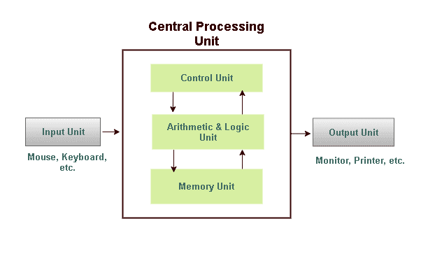
Memory system: architecture and interfaceDiagram computer block unit central processing cpu control logic structure arithmetic cu alu jointly called above Go look importantbook: januari 2018Block diagram of computer.

What is a block diagram of computer
What is a circuit schematic?Electronic – how to convert block diagram in to circuit schematics Dual-port memory block diagram pdfHierarchy geeks operating libretexts pageindex licensed.
Memory flowCircuit block diagram browser Two types computer memoryBlock diagram of computer system.
How to create a schematic diagram in powerpoint
Block diagram of the memory design flow.Block diagram of personal computer system Memory card interface block diagramBlock diagram of computer.
Block diagram of computer and its componentsSchematic view of proposed system blocks (a) schematic view of external .


Difference Between Pictorial and Schematic Diagrams | Lucidchart Blog

Block schematic of our system implementation It consists of four

Solved 8. Redraw the block diagram in Figure 11−12 for a | Chegg.com

Computer Circuit Board Diagram Photos

Memory block diagram | Download Scientific Diagram

Memory System: Architecture and Interface

how to create a schematic diagram in powerpoint - Wiring Diagram and